International Journal of Mechanical Engineering and Mechatronics (IJMEM)
ISSN: 1929-2724

Volume 1, Issue 2 Year 2012 - Pages 61-65
DOI: 10.11159/ijmem.2012.007
A New Experimental Method to Obtain the Ion Beam Profile of Focused Ion Beam Nanotechnology Systems
José Anguita, Raquel Alvaro, Francisco Espinosa
Instituto de Microelectrónica de Madrid (CSIC)
Isaac Newton 8, 28760 Tres Cantos Madrid, Spain
anguita@imm.cnm.csic.es
Abstract - An experimental method is proposed to measure the exact size of the ion beam produced by a liquid metal Ga ion source in Focused Ion Beam systems. This method involves the fabrication of arrays of trenches having different periods, followed by Atomic Force Microscope measurements and further uncomplicated calculations. This method gives the ion beam profile in terms of beam current density at any distance from the centre of the beam and with a resolution in the range of a few nanometres. The method proposed in this paper shows that the beam size measured by the classical sweeping across a knife edge method is several times smaller than the exact size and therefore it is not directly related with the real resolution of the fabrication system, especially when dealing with low ion beam current levels suitable for nanotechnology. At an ion beam current of 1 pA, the tail region widens the beam to 30 nm from its centre, imposing limits to the resolution in terms of minimum period that is expected taking into account only the core part of the ion beam.
Keywords: Nanotechnology, Focused Ion Beam, Liquid Metal Ga ion source, Ion Beam Profile.
© Copyright 2012 Authors - This is an Open Access article published under the Creative Commons Attribution License terms. Unrestricted use, distribution, and reproduction in any medium are permitted, provided the original work is properly cited.
1. Introduction
The concept of resolution of a manufacturing system is very important, especially when it is referred to a nanofabrication tool. In top-down nanofabrication technologies, elements have to be not only very small, but also be placed very close to each other. In many cases a manufacturing system can deal with small sizes but not with very small separations. A typical example is found in Electron Beam Lithography (EBL) systems where the distance between elements is much lower than the expected from the diameter of the electron beam due to the forward and backward scatterings in both the resist layer and the substrate.
Because Focused Ion Beam (FIB) systems does not require any resist layer (Ampere, 2004, Langford et al., 2007), it can be used in cases where EBL systems are unable to place elements very close to each other. However, in FIB systems is found that the minimum distance between elements is larger than the expected from the core part size of the ion beam. This is due to the tail part of the electrical current distribution of the ion beam in a focusing column suffering from distortions (Rempfer and Mauck, 1988). Therefore, it is necessary to know the sizes of the core and the tail parts tail of the ion beam in a FIB system in order to determine its real possibilities in nanofabrication.
Previous works by other authors to measure the ion beam size are based on the sweeping the beam across a knife edge method. In this method, the ion beam is scanned across a metallic sharp knife edge and recording the intensity of the secondary electron current at every position of the ion beam. The distance between the positions of the beam at which the integrated current profile is the15% and the 85% of the maximum determines the ion beam size (Orloff and Sato, 1991). However, other studies have demonstrated that this method suffers from errors when it is applied to very low ion current beams (~ 1 pA). These errors are in particular due to uncertainties arising from a high noise level resulting from ion beam electrical currents levels several times smaller than the normal current levels. In these studies, the authors use other methods to measure the actual sizes of an ion beam. These methods are based on: mechanical probes that are placed between the beam and the target (Gabriel Lopes et al., 2011, Sosolik et al., 2000) which don't provide very low resolution specially when dealing with low ion beam currents (~ 1 pA), or on exposing a target to the ion beam and measuring the damage done to it (Wang and Wang 1996, Park et al. 2004) which requires complicated samples preparation and not standard instrumentation equipment for AES analysis to obtain the Ga concentration profiles in the parallel direction to the incident beam, or on mathematical simulation being the ion beam approximated by a Gaussian distribution (Petit et al., 2005 and Orloff et al. 1991).
We present in this paper a new experimental method to measure the ion beam profile in terms of beam current density at any distance from the centre of an ion beam with a resolution of few nanometres. This method implies the fabrication by FIB of several arrays of trenches having different periods of values ranging from larger to smaller than the expected diameter of the ion beam. A special scan technique during the fabrication of the arrays of trenches has to be used in order to prevent the formation of oblique planes at the bottom and top of the trenches. This is followed by measurement of the depth of the trenches by Atomic Force Microscope (AFM) that has to be dotted with a special tip having a very small curvature radius. Finally, uncomplicated calculations have to be done. The method is applied to the ion beam current of a FIB system carrying a current of 1 pA.
2. Arrays Fabrication and AFM Measurements
2. 1. Experimental
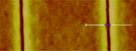
We have used a FIB dotted with a new patented liquid metal Ga ions source with an apex radius less than 10 microns. It has only one column (the one for the ion beam) with electrostatic optic elements (lens and deflectors) and a high quality secondary electrons detector. The column has a fast ion beam blanker that is activated to measure the ion beam current. Ions are then directed to a Faraday cup connected to a pico-ammeter. Focusing and astigmatism correction are made by sputtering the silicon surface during 3 seconds at a magnification of 200K, near the writing field where the array of trenches are going to be fabricated. The created crater is visualised and the quality of its image is optimised by changing the working distance. At the same time, the astigmatism corrections is made by wobbling the image of the crater and adjusting the aperture position until the image becomes sharp during the wobbling with not shift in X or Y direction. Final astigmatism correction is made by further focusing using the settings of the stigmator lens. Focusing and astigmatism correction are finished when the upper part of the crater is a perfect circle with a diameter of less than 50 nm
The values of the etching parameters are: ion energy 30 keVs, length of the trenches in the arrays 10 µm, step size of the beam during the scans 1 nm, ion beam current 1 pA, line dose 10 nC/cm equivalent to an etching time of 10 ms per trench, and array periods from 65 nm down to 20 nm with also some isolated trenches. The number of trenches in the array (width of the array) was selected so that the total fabrication time for every array was less than 0.5 seconds and therefore the mechanical and thermal stage drift with time was negligible (Petit et al., 2005). The total dose was supplied in 100 scans (etched depth/scan ~ 0.16 nm), thus avoiding the appearing of stepped surfaces at the bottom and top of the trenches from scan to scan and so the possible variation of the sputtering yield of the Ga+ ions arriving to the target with the incident angle (Qiangmin Wei et al.). They report that for incident angle less than 10o relative to the normal to the target, the sputtering yield is practically the same as at 0o. In our case, due to the mentioned technique of scanning, this angle is always less than 4o at the bottom and top of the trenches. These parts of the trenches are crucial for the proposed method in this paper.
For AFM measurements, we have used a nanoScope V from Veeco (Webb-1), dotted with a special tip having a curvature radius of 2 nm. The step size of the probe during the measures was 1 nm. This ensures a minimum error in the measures of the depth of the trenches.
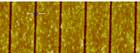
As material for etching, we have used a 20 nm thick layer of Platinum deposited by sputtering. The reason why we have used Platinum instead of a more common material such as silicon can be understood by observing the figure 1.
When platinum is used (figure 1a), the surface next to the trench has the original roughness of the material.
 (a)
(a)
 (b)
(b)
 (c)
(c)
 (d)
(d)
However when silicon is used (figure 1b), the surface next to the line shows a large roughness with peaks-shapes of about 1.5 nm above de original silicon surface. These peaks are due to the classical redeposition of the backscattered silicon particles from the trench as a result of a pure physical silicon etching mechanism. The higher mean free path of the backscattered platinum particles from the trench avoids redeposition of the etched platinum into the trenches, allowing the trenches to be placed closer to each other and therefore it is possible to use periods smaller than the diameter of the ion beam; this is essential to obtain the ion beam profile as it will be shown later in the paper. For a line dose of 10 nC/cm, the etched depth in platinum is 16 nm as measured in the resulting isolated trenches (500 nm apart). This value will be used as a reference in the next sections.
2. 2. Topography Results
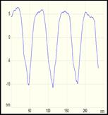
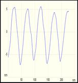
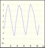
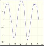
Figure 2 shows the results of the AFM measurements on the fabricated arrays with periods of 65 nm (a), 50 nm (b), 35 nm (c), and 25 nm (d). All the trenches in the arrays have been etched with the same dose of 10 nC/cm.
For the array with period of 65 nm, the measured depth of the trenches is 16 nm, just the same as in the case of isolated trenches, and it is also observed that the surface between the trenches is still flat. However, for the array having a period of 50 nm, the depth is reduced to 11 nm, and the surface between the trenches appears rounded. These differences are more pronounced when the period is 35 nm where the depth of the trenches is 5 nm, and even more pronounced when the period is 25 nm with a depth of only 2.4 nm. Because the desired depth of the trenches in the arrays is 16 nm, we can conclude that the resolution in terms of minimum period of this particular FIB system is about 60 nm at a current level of 1 pA when the etched surface is 16 nm.
 (a)
(a)
 (b)
(b)
 (c)
(c)
 (d)
(d)
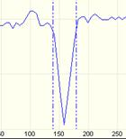
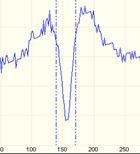
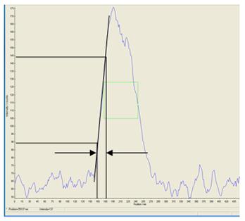
On the other hand, figure 3 shows the image obtained by sweeping the ion beam across a knife edge. To get this figure, the 1 pA ion beam is swept in steps of 1 nm across a platinum nano-particle close to the working areas where the arrays are going to be patterned. The secondary electron current intensity produced by the sweeping is registered at every position of the ion beam. The 15%-85% points on the integrated current profile shown in figure 3 indicate that the beam diameter is about 15 nm. Therefore it would be expected that the width of the trenches should be about 15 nm and width a minimum period a bit longer than that value. However the actual resolution in terms of minimum period is about 60 nm as it can be deduced from the depth measurement of the trenches in the array of period 65 nm which value is 16 nm. In the next section we are going to analyze the reason for this decrease in the depth of the trenches as the period of the arrays is reduced, and also how it is possible to obtain the ion beam profile from the data shown in figure 2.
3. Analysis about the Reduction in Depths of the Arrays
When the period of the array of trenches is larger than the ion beam diameter (D), each trench is etched as if it was isolated from the rest of the trenches, and the original platinum surface is still between the trenches as shown in figure 2a. However when the period is smaller than the ion beam diameter, the beams overlap each other at the etch positions as shown in figure 4. The platinum at the centre of the overlapping areas is also etched at a rate that depends on the electrical current density at that point, resulting in a reduction (H) in the depth respect to the original platinum surface and therefore the depth of the trenches in the array is (16-H) nm, or in other words, H=16-depth.
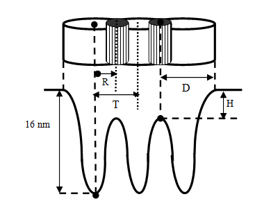
We have fabricated arrays with different periods (T) and we have measured by AFM the value of the depths as previously shown in figure 2, thus getting the H values for every period. Note that H corresponds to the platinum that is etched at the centre of the overlapping region which is located at a distance R from the centre of the ion beam, being R equals to half of the period T. The different values of H with the period T of the array are given in Table 1.
Table 1. Values of the depth of the trenches and H=(16-depth) of every array with its period.
|
Period (nm) |
Depth (nm) |
H (nm) |
|
60 |
16 |
0 |
|
50 |
11.5 |
4.5 |
|
40 |
7.0 |
9.0 |
|
35 |
5.4 |
10.6 |
|
30 |
4.2 |
11.8 |
|
25 |
2.4 |
13.6 |
|
20 |
1.0 |
15 |
If we normalized the ion beam current density at its centre (J=1), thus resulting in an etch depth of 16 nm, the current density at a distance R=T/2 from the centre is given by J(T/2)=H/(16x2)=H/32, taken into account here that the platinum is etched twice in the overlapping area (by the beam at any position and at the position immediately to its right) and that the depth is directly proportional to the beam current given that any redeposition of the etched platinum into the trench is observed (see figure 1a). So for instance, according to the array with period T=50 nm (figure 2b), the depth of the trenches is 11.5 nm, thus resulting in R=25 nm, H=4.5 nm, and J=0.14, and also according to the array with period T=25 nm (figure 2d), the depth of the trenches is 2.4 nm, thus resulting in R=12.5 nm, H=13.6 nm, and J=0.425.
In this figure, for the normalized ion beam density at R=5.0 nm, and R = 7.5 nm we have used an approximation that consists on the following. Due to the small roughness of the initial platinum layer and the small value of the depth of trenches of the arrays with period T= 10 nm and 15 nm, we were not completely sure about the error of the measurements of the depth of the trenches. Therefore, for the data at R=7.5 nm we have used the extrapolation of the ion beam current density data for R longer than 20 nm. For R=5 nm we have taken into account the information extracted from the figure 3.
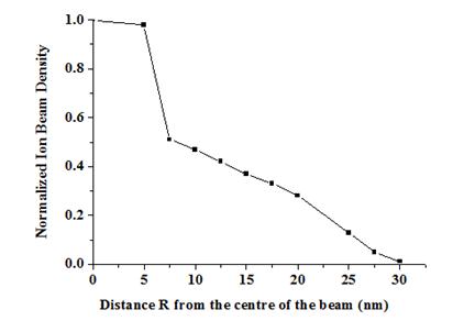
We can note that the beam is composed of two parts, the core and the tail regions which are clearly different. The core part extends to about 7.5 nm from the beam centre (thus resulting in a main diameter of about 15 nm), while the tail region extends from the edge of the core to approximately 25 nm beyond (thus resulting in a beam diameter of about 60 nm). The core part of the beam carries most of the ion current and it seems that it takes the information of the beam size measured by the sweeping across a knife edge method (see figure 3). Due to the low value of the ion beam current used here (1 pA), the information carried within the tail region of the ion beam is discarded from the region outside the 15%-85% points region. However it has been shown that the tail region is responsible for widening the top part of the trenches as shown in figure 2b, thus avoiding the closer placement of trenches and resulting a minimum period of about 60 nm as shown in figure 2a in our arrays.
4. Conclusion
An experimental method is proposed to measure the exact size of the ion beam produced by a liquid metal Ga ion source in Focused Ion Beam systems. This method involves the fabrication of arrays of trenches having different periods, followed by Atomic Force Microscope measurements and further uncomplicated calculations. This method gives the ion beam profile in terms of beam current density at any distance from the centre of the beam and with a resolution of a few nanometres. The method proposed in this paper shows that the beam size measured by the classical sweeping across a knife edge method is several times smaller than the exact size and therefore it is not directly related with the real resolution interns of the minimum possible period of the fabrication system, especially when dealing with low ion beam current levels suitable for nanotechnology. At an ion beam current of 1 pA, the tail region widens the beam to 30 nm from its centre, imposing limits to the resolution in terms of minimum period that is expected taking into account only the core part of the ion beam.
Acknowledgements
Jose Anguita acknowledges funding support from the CAM (Comunidad Autonoma de Madrid, "NANOBIOMAGNET" project), Raquel Alvaro from the Spanish MICINN (fellowship), and Francisco Espinosa from the CSIC (JAE fellowship).
References
Ampere, A. T. (2004). Recent developments in micromillingusing focused ion beam technology. Journal of Microme-chanics and Microengineering, 14, R15–R34. View Article
Gabriel Lopes, J., Rocha, J., Redondo, L. M., Corrêa Alegria, F.(2011). High resolution ion beam profilemeasurement system. Proceedings of ICALEPCS2011,Grenoble, France, 164-167. View Article
Langford, R. M., Nellen, P. M., Gierak, J., Fu, Y. (2007). Focusedion beam micro-and nanoengineering. MRS BULLETIN, 32, 417-423. View Article
Orloff, J., Li, J. Z., Sato, M. (1991). Experimental study of a focused ion beam probe size and comparison with theory. Journal of Vacuum Science and Technology, B9, 2609-2612. View Article
Park, C. M., Bain, J. A., Clinton, T. W., van der Heijden, P. A. A.,Klemmer, T. J. (2004). Measurement of Ga implantation profiles in the sidewall and bottom of focused-ion-beam-etched structures. Applied Physics Letters, 84, 3331-3334. View Article
Petit, P., Faulkner, C. C., Johnstone, S., Wood, D., Cowburn, R. P. (2005). Nanometer scale patterning using focused ion beam milling. Review of Scientific Instruments, 76, 026105 View Article
Qiangmin, W., Kun-Dar, L., Lian, J., Wang, L. (2008). Angular dependence of sputtering yield of amorphous and polycrystalline materials. Journal of Physics D: Applied Physics 41(17):172002 View Article
Rempfer, G. F., Mauck, M. S. (1988). A closer look at the effect of lens aberrations and object size on the intensity distribution and resolution in electron optics. Journal of Applied Physics, 63, 9, 2187-2199. View Article
Sosolik, C. E., Lavery, A. C., Dahl, E. B., Coope, B. H. (2000), Atechnique for accurate measurements of ion beamcurrent density using a Faraday cup. Review of Scientific Instruments, 71, 3326-3330 View Article
Wang, J. B., Wang, Y. L. (1996). A novel procedure formeasuring the absolute current density profileof a focused gallium-ion beam. Applied PhysicsLetters, 69, 2764-2767. View Article
Website References
Nanoscale Enzyme Therapy - News Item, Consulted on 5 September 2012 View Website